


Industry
ESD flooring for semiconductor and fab
Wafer handling, probe and assembly sit inside a controlled environment where the floor has to satisfy a particle class and a resistance band at once.[1]
What is different about these rooms
Two specifications, one slab
ISO 14644-1 classification and an ESD resistance band are independent requirements. The class does not set the band and the band does not set the class.
Cleaning regimes fight ESD performance
A finish applied for particulate reasons sits between the floor and the ground path. The cleaning contract has to be written alongside the ESD program.
Tool moves are the wear pattern
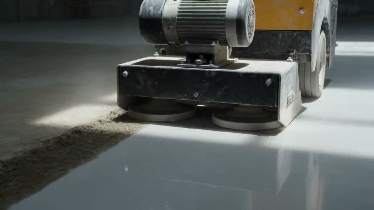
Equipment install and moves abrade specific lanes hard. Those lanes are where the floor drops out of band first, so they are where reverification should focus.

Sources
- ANSI/ESD S20.20-2021, the ESD control program standard for electronics handling
ESD control program requirements (administrative and technical) for any organization that handles ESD-sensitive electrical or electronic parts.
www.esda.org - Conductive and dissipative ESD epoxy technical data sheet, resistance and cure figures
Cited here for the conductive flooring/coating resistance band. The ESD Association's own consumer-facing page states only the <= 1.0 x 10⁶ ohm ceiling with no stated floor.
www.arcat.com
Every number on this page came from one of those documents. Send us the room and we will tell you which of them your floor has to answer to.